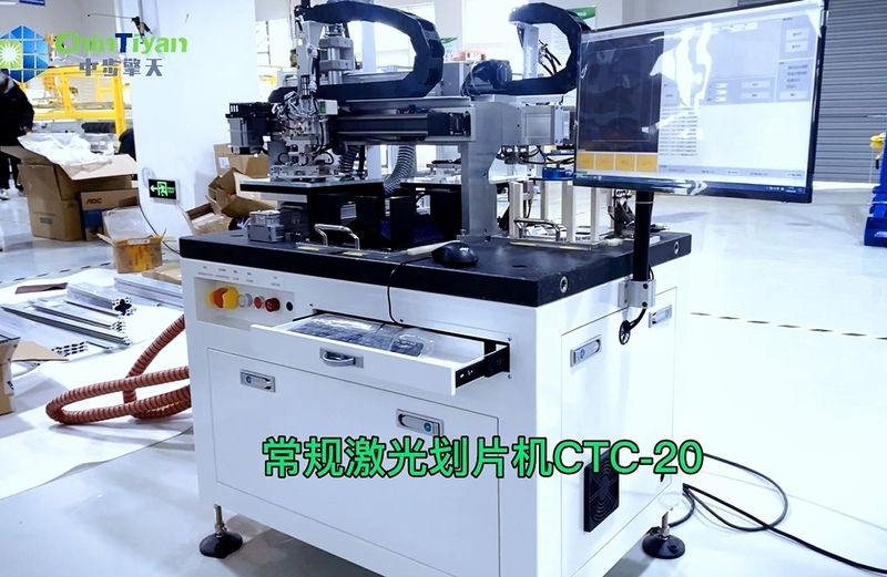
The principle and function of battery cell laser slicerIssuing time:2024-03-14 16:13 一、 The working principle of high-speed laser non-destructive cutting machine for photovoltaic cells:
1. The high-speed laser non-destructive cutting machine for photovoltaic cells uses a high-energy laser beam to irradiate the surface of the cell or silicon wafer, causing local melting and gasification in the irradiated area. Under the drive of a CNC worktable, laser cutting is carried out to achieve the purpose of cutting. 2. Laser cutting has high energy density and good cutting effect, and its processing is non-contact, without mechanical impact on the battery/silicon wafer itself, making it less prone to damage and breakage. 3.Furthermore, due to the minimal thermal impact and high cutting accuracy of laser cutting, it is widely used in the photovoltaic industry for cutting solar cells and silicon wafers. 二、 What are the functions of the battery cell laser slicer: The solar cell laser slicer is a high-precision equipment that uses laser technology to crack silicon wafers. Laser cutting is used on silicon wafers to create cracks, thereby achieving the segmentation and processing of silicon wafers. In the solar energy industry, slicing and cutting of single crystal silicon and polycrystalline silicon with rounded corners or edges on all four sides. Separation and cutting of monocrystalline silicon and polycrystalline silicon wafers in the electronics industry. The solar cell laser slicer can achieve precise cracking of silicon wafers, ensuring that the size and shape of the shards meet the requirements. The solar cell laser slicer has efficient production capacity, which can greatly improve production efficiency and capacity. The equipment integrates various advanced automation technologies such as PLC, laser, sensor, servo, etc., to achieve fully automatic processing of silicon wafer loading, detection, slicing, unloading and boxing. The unique mechanical structure design and process make the edges of silicon wafers smooth and the surface dust-free after slicing. 聲明:此篇為中步擎天原創(chuàng),轉(zhuǎn)載請(qǐng)標(biāo)明出處鏈接:http://www.npcnn.cn/en/sys-nd/52.html
|


